

Veja as especificações para detalhes do produto.
EP2AGX125DF25C5NES
Product Overview
Category
EP2AGX125DF25C5NES belongs to the category of Field Programmable Gate Arrays (FPGAs).
Use
FPGAs are integrated circuits that can be programmed or reprogrammed after manufacturing. They are widely used in various electronic applications, including telecommunications, automotive, aerospace, and consumer electronics.
Characteristics
- EP2AGX125DF25C5NES is a high-performance FPGA designed for complex digital designs.
- It offers a large number of logic elements, memory blocks, and high-speed transceivers.
- The device supports advanced features such as embedded processors, high-speed serial interfaces, and DSP blocks.
- It provides flexibility and scalability, allowing designers to implement custom logic functions.
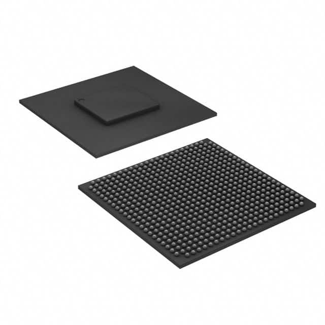
Package
EP2AGX125DF25C5NES comes in a compact package suitable for surface mount technology (SMT) assembly.
Essence
The essence of EP2AGX125DF25C5NES lies in its ability to provide a programmable hardware platform for implementing complex digital systems.
Packaging/Quantity
The specific packaging and quantity information can vary depending on the manufacturer and distributor. Please refer to the product documentation or contact the supplier for detailed information.
Specifications
- Logic Elements: 125,000
- Memory Blocks: 4,608
- Embedded Multipliers: 648
- High-Speed Transceivers: 24
- Maximum User I/Os: 622
- Operating Voltage: 1.2V
- Operating Temperature Range: -40°C to 100°C
- Package Type: BGA (Ball Grid Array)
- Package Pin Count: 1152
Detailed Pin Configuration
For the detailed pin configuration of EP2AGX125DF25C5NES, please refer to the official datasheet provided by the manufacturer. The datasheet contains comprehensive information about the pin assignments, functions, and electrical characteristics.
Functional Features
EP2AGX125DF25C5NES offers several functional features that enhance its performance and versatility:
- High Logic Capacity: With 125,000 logic elements, the FPGA can accommodate complex designs and perform advanced computations.
- Embedded Processors: The device supports embedded processors, allowing for the integration of software and hardware functionalities.
- High-Speed Transceivers: The FPGA includes 24 high-speed transceivers, enabling fast data communication between different components.
- DSP Blocks: Dedicated Digital Signal Processing (DSP) blocks provide efficient implementation of mathematical operations commonly used in signal processing applications.
- Flexible I/O Options: EP2AGX125DF25C5NES offers a wide range of user I/Os, providing flexibility for connecting external devices and peripherals.
Advantages and Disadvantages
Advantages
- Versatility: EP2AGX125DF25C5NES can be programmed to perform various tasks, making it suitable for a wide range of applications.
- Scalability: The FPGA's large logic capacity and memory blocks allow for scalable designs.
- Reconfigurability: The ability to reprogram the FPGA enables design modifications without changing the hardware.
- High Performance: The device offers high-speed transceivers and DSP blocks, enhancing its computational capabilities.
Disadvantages
- Complexity: Working with FPGAs requires specialized knowledge and expertise.
- Power Consumption: FPGAs can consume more power compared to other integrated circuits.
- Cost: FPGAs tend to be more expensive than fixed-function integrated circuits.
Working Principles
EP2AGX125DF25C5NES operates based on the principles of digital logic. It consists of configurable logic blocks, interconnect resources, and input/output interfaces. The logic blocks can be programmed to implement desired logic functions, while the interconnect resources facilitate communication between different blocks. The input/output interfaces allow the FPGA to interact with external devices.
The device can be programmed using Hardware Description Languages (HDLs) such as VHDL or Verilog. The programming code describes the desired functionality and is then synthesized into a configuration file that can be loaded onto the FPGA.
Detailed Application Field Plans
EP2AGX125DF25C5NES finds applications in various fields, including:
- Telecommunications: The FPGA can be used in base stations, network switches, and routers to handle high-speed data processing and protocol conversions.
- Automotive: It can be employed in advanced driver assistance systems (ADAS), engine control units (ECUs), and infotainment systems for enhanced performance and flexibility.
- Aerospace: FPGAs are utilized in satellite communication systems, avionics, and radar systems due to their ability to handle complex algorithms and high-speed data processing.
- Consumer Electronics: The device can be integrated into smart TVs, gaming consoles, and wearable devices to enable advanced functionalities and customization options.
Detailed and Complete Alternative Models
There
Liste 10 perguntas e respostas comuns relacionadas à aplicação de EP2AGX125DF25C5NES em soluções técnicas
Sure! Here are 10 common questions and answers related to the application of EP2AGX125DF25C5NES in technical solutions:
1. What is EP2AGX125DF25C5NES? EP2AGX125DF25C5NES is a specific model of Field-Programmable Gate Array (FPGA) manufactured by Intel.
2. What are the key features of EP2AGX125DF25C5NES? Some key features of EP2AGX125DF25C5NES include high-density programmable logic, embedded memory blocks, high-speed transceivers, and support for various I/O standards.
3. What are the typical applications of EP2AGX125DF25C5NES? EP2AGX125DF25C5NES is commonly used in applications such as telecommunications, networking, industrial automation, video processing, and high-performance computing.
4. How can EP2AGX125DF25C5NES be programmed? EP2AGX125DF25C5NES can be programmed using Hardware Description Languages (HDLs) such as VHDL or Verilog, along with design software provided by Intel.
5. What is the maximum number of logic elements in EP2AGX125DF25C5NES? EP2AGX125DF25C5NES has a maximum capacity of 125,000 logic elements, which can be used to implement complex digital circuits.
6. Does EP2AGX125DF25C5NES support high-speed data transfer? Yes, EP2AGX125DF25C5NES supports high-speed data transfer through its built-in transceivers, enabling communication at rates up to several gigabits per second.
7. Can EP2AGX125DF25C5NES interface with external devices? Yes, EP2AGX125DF25C5NES supports various I/O standards and can interface with external devices such as sensors, memory modules, and communication interfaces.
8. Is EP2AGX125DF25C5NES suitable for real-time signal processing? Yes, EP2AGX125DF25C5NES is well-suited for real-time signal processing applications due to its high-performance capabilities and support for parallel processing.
9. Can EP2AGX125DF25C5NES be reprogrammed after deployment? Yes, EP2AGX125DF25C5NES is a reprogrammable FPGA, allowing for updates or modifications to the implemented logic even after the device has been deployed.
10. Are there any development kits available for EP2AGX125DF25C5NES? Yes, Intel provides development kits and evaluation boards specifically designed for EP2AGX125DF25C5NES, which include necessary software tools and documentation for easier prototyping and development.
Please note that the specific details and answers may vary depending on the context and requirements of the technical solution.