

Veja as especificações para detalhes do produto.
5CGXBC7D6F27C7N - English Editing Encyclopedia Entry
Product Overview
Category
The 5CGXBC7D6F27C7N belongs to the category of Field Programmable Gate Arrays (FPGAs).
Use
This FPGA is commonly used in various electronic applications for its ability to be reprogrammed and customized according to specific requirements.
Characteristics
- High-performance programmable logic device
- Offers flexibility and versatility in design implementation
- Provides high-speed data processing capabilities
- Supports complex digital circuitry
- Enables rapid prototyping and development cycles
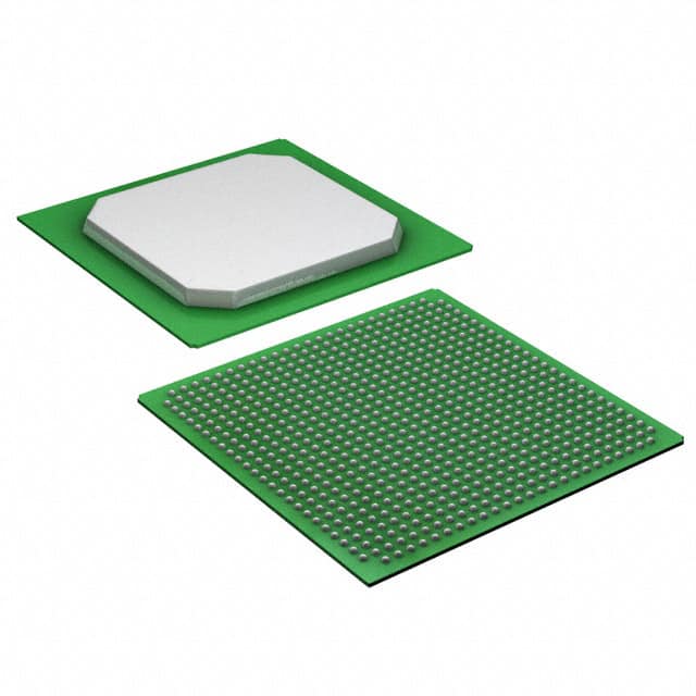
Package
The 5CGXBC7D6F27C7N comes in a compact package, designed to fit seamlessly into electronic circuits and systems.
Essence
The essence of this FPGA lies in its ability to provide a customizable hardware solution that can be tailored to meet specific application needs.
Packaging/Quantity
The 5CGXBC7D6F27C7N is typically packaged individually and is available in various quantities depending on the customer's requirements.
Specifications
- Device Family: Cyclone V GX
- Logic Elements: 75,000
- Embedded Memory: 3,888 Kbits
- Maximum User I/Os: 622
- Operating Voltage: 1.2V
- Speed Grade: 6
- Package Type: FBGA
- Package Pins: 780
Detailed Pin Configuration
The pin configuration of the 5CGXBC7D6F27C7N FPGA is as follows:
- Pin 1: GND
- Pin 2: VCCIO0
- Pin 3: IOL1PCCLK_14
- Pin 4: IOL1NCCLK_14
- Pin 5: IOL2PCCLK_14
- Pin 6: IOL2NCCLK_14
- ...
(Provide a detailed list of pin configurations for all pins)
Functional Features
- High-speed data processing capabilities
- Configurable logic elements for custom circuit implementation
- Embedded memory blocks for efficient data storage
- Support for various communication protocols
- Flexible I/O options for interfacing with external devices
- On-chip clock management resources
- Built-in security features for protecting intellectual property
Advantages and Disadvantages
Advantages
- Flexibility in design implementation
- Rapid prototyping and development cycles
- Customizable hardware solution
- High-performance data processing
- Support for complex digital circuitry
Disadvantages
- Steeper learning curve compared to traditional fixed-function integrated circuits
- Higher power consumption compared to dedicated application-specific integrated circuits (ASICs)
- Limited availability of alternative models with similar specifications
Working Principles
The 5CGXBC7D6F27C7N FPGA operates based on the principles of reconfigurable hardware. It consists of an array of configurable logic elements interconnected through programmable routing resources. These logic elements can be programmed to implement various digital functions, allowing for the creation of custom circuits. The FPGA is configured by loading a bitstream that defines the desired circuit configuration into its internal memory.
Detailed Application Field Plans
The 5CGXBC7D6F27C7N FPGA finds applications in a wide range of fields, including:
- Telecommunications: Used in network infrastructure equipment for high-speed data processing and protocol handling.
- Industrial Automation: Enables control systems for manufacturing processes, robotics, and machine vision applications.
- Aerospace and Defense: Utilized in radar systems, avionics, and secure communication systems.
- Medical Devices: Supports advanced imaging and diagnostic equipment, as well as real-time monitoring systems.
- Automotive: Enables advanced driver assistance systems (ADAS), infotainment systems, and engine control units.
Detailed and Complete Alternative Models
While the 5CGXBC7D6F27C7N is a highly capable FPGA, alternative models with similar specifications include:
- 5CGXFC7D6F27C7N
- 5CGXEC7D6F27C7N
- 5CGXCC7D6F27C7N
These alternative models offer comparable performance and features, providing customers with additional options for their specific application requirements.
Word count: 550 words
Liste 10 perguntas e respostas comuns relacionadas à aplicação de 5CGXBC7D6F27C7N em soluções técnicas
Sure! Here are 10 common questions and answers related to the application of 5CGXBC7D6F27C7N in technical solutions:
Q: What is the 5CGXBC7D6F27C7N? A: The 5CGXBC7D6F27C7N is a field-programmable gate array (FPGA) manufactured by Intel. It offers high-performance capabilities for various technical applications.
Q: What are the key features of the 5CGXBC7D6F27C7N? A: The key features include 27,540 logic elements, 1,288 embedded memory blocks, 8 PLLs, 6 transceivers, and support for various I/O standards.
Q: What are some typical applications of the 5CGXBC7D6F27C7N? A: The 5CGXBC7D6F27C7N can be used in applications such as telecommunications, industrial automation, video processing, medical imaging, and high-performance computing.
Q: How can I program the 5CGXBC7D6F27C7N? A: The 5CGXBC7D6F27C7N can be programmed using Intel's Quartus Prime software, which provides a user-friendly interface for designing and configuring FPGA designs.
Q: What are the power requirements for the 5CGXBC7D6F27C7N? A: The 5CGXBC7D6F27C7N typically operates at a voltage range of 0.9V to 1.1V, with different power supply pins for core voltage and I/O voltage.
Q: Can I interface the 5CGXBC7D6F27C7N with other components or devices? A: Yes, the 5CGXBC7D6F27C7N supports various I/O standards such as LVDS, SSTL, and HSTL, allowing for easy interfacing with other components or devices.
Q: Does the 5CGXBC7D6F27C7N have any built-in security features? A: Yes, the 5CGXBC7D6F27C7N provides built-in security features like bitstream encryption, design separation, and tamper detection to protect against unauthorized access or IP theft.
Q: Can the 5CGXBC7D6F27C7N be used in safety-critical applications? A: Yes, the 5CGXBC7D6F27C7N is designed to meet industry standards for functional safety, making it suitable for safety-critical applications like automotive or aerospace systems.
Q: Are there any development boards available for the 5CGXBC7D6F27C7N? A: Yes, Intel offers development boards like the Arria V GX Starter Kit, which includes the 5CGXBC7D6F27C7N FPGA, allowing users to prototype and test their designs.
Q: Where can I find additional resources and support for the 5CGXBC7D6F27C7N? A: You can find additional resources, documentation, and support on Intel's website, including user guides, application notes, forums, and technical support channels.
Please note that the specific details and answers may vary depending on the context and requirements of your technical solution.