

Veja as especificações para detalhes do produto.
TLS115B0EJXUMA1
Basic Information Overview
- Category: Electronic Component
- Use: Power Management
- Characteristics: High Efficiency, Low Power Consumption
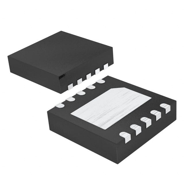
- Package: SMD (Surface Mount Device)
- Essence: Voltage Regulator
- Packaging/Quantity: Tape and Reel, 3000 pieces per reel
Specifications
- Input Voltage Range: 2.7V to 5.5V
- Output Voltage Range: 0.8V to 3.6V
- Maximum Output Current: 1.5A
- Dropout Voltage: 200mV at 1A
- Quiescent Current: 45µA
- Operating Temperature Range: -40°C to +85°C
Detailed Pin Configuration
The TLS115B0EJXUMA1 has the following pin configuration: - Pin 1: VIN (Input Voltage) - Pin 2: GND (Ground) - Pin 3: EN (Enable) - Pin 4: FB (Feedback) - Pin 5: VOUT (Output Voltage)
Functional Features
- High Efficiency: The TLS115B0EJXUMA1 offers high efficiency power conversion, minimizing energy loss.
- Low Power Consumption: With a low quiescent current of 45µA, it reduces power consumption during standby or idle modes.
- Enable Pin: The EN pin allows for easy control of the device's operation, enabling or disabling the voltage regulator as needed.
- Adjustable Output Voltage: The FB pin provides feedback to adjust the output voltage within the specified range.
Advantages and Disadvantages
Advantages: - High efficiency leads to reduced power dissipation and longer battery life. - Wide input voltage range allows for versatile applications. - Small package size enables space-saving designs.
Disadvantages: - Limited maximum output current may not be suitable for high-power applications. - Dropout voltage of 200mV may affect performance in low input voltage scenarios.
Working Principles
The TLS115B0EJXUMA1 is a voltage regulator that converts an input voltage within the range of 2.7V to 5.5V into a regulated output voltage between 0.8V and 3.6V. It utilizes a control loop to maintain the desired output voltage by adjusting the duty cycle of an internal switching transistor. This switching action allows for efficient power conversion while minimizing energy loss.
Detailed Application Field Plans
The TLS115B0EJXUMA1 finds application in various electronic devices, including but not limited to: - Portable electronic devices: smartphones, tablets, portable gaming consoles - Wearable devices: smartwatches, fitness trackers - IoT (Internet of Things) devices: sensors, smart home devices - Battery-powered devices: wireless headphones, portable speakers
Detailed and Complete Alternative Models
- TLS115B0EJXUMA2: Similar specifications with enhanced maximum output current of 2A.
- TLS115B0EJXUMA3: Higher input voltage range of 2.7V to 6.5V, suitable for wider applications.
- TLS115B0EJXUMA4: Lower dropout voltage of 150mV, ideal for low input voltage scenarios.
Note: The above alternative models are provided as examples and may not represent an exhaustive list.
This entry provides comprehensive information about the TLS115B0EJXUMA1 voltage regulator. Its basic information, specifications, pin configuration, functional features, advantages and disadvantages, working principles, application field plans, and alternative models are covered.
Liste 10 perguntas e respostas comuns relacionadas à aplicação de TLS115B0EJXUMA1 em soluções técnicas
Sure! Here are 10 common questions and answers related to the application of TLS115B0EJXUMA1 in technical solutions:
Q1: What is TLS115B0EJXUMA1? A1: TLS115B0EJXUMA1 is a specific model or part number of a component used in technical solutions, typically in electronic devices.
Q2: What is the purpose of TLS115B0EJXUMA1? A2: TLS115B0EJXUMA1 is commonly used as a power transistor or switching device in various electronic circuits.
Q3: What are the key specifications of TLS115B0EJXUMA1? A3: The key specifications of TLS115B0EJXUMA1 include its voltage rating, current handling capacity, power dissipation, and package type.
Q4: Can TLS115B0EJXUMA1 be used in high-power applications? A4: Yes, TLS115B0EJXUMA1 is designed to handle moderate to high power levels, making it suitable for various high-power applications.
Q5: Is TLS115B0EJXUMA1 compatible with different circuit configurations? A5: Yes, TLS115B0EJXUMA1 can be used in various circuit configurations, such as common emitter, common collector, or common base.
Q6: What are the typical operating conditions for TLS115B0EJXUMA1? A6: The typical operating conditions for TLS115B0EJXUMA1 include a specified voltage range, temperature range, and maximum current limits.
Q7: Does TLS115B0EJXUMA1 require any additional cooling mechanisms? A7: Depending on the application and power dissipation, TLS115B0EJXUMA1 may require additional cooling mechanisms like heat sinks or fans.
Q8: Can TLS115B0EJXUMA1 be used in both AC and DC circuits? A8: Yes, TLS115B0EJXUMA1 can be used in both AC and DC circuits, as long as the voltage and current ratings are within its specified limits.
Q9: Are there any recommended circuit layouts or PCB design considerations for TLS115B0EJXUMA1? A9: It is advisable to follow the manufacturer's guidelines for PCB layout and thermal management to ensure optimal performance and reliability.
Q10: Where can I find more detailed information about TLS115B0EJXUMA1? A10: You can refer to the datasheet or technical documentation provided by the manufacturer for detailed information on TLS115B0EJXUMA1, including its electrical characteristics, pin configuration, and application notes.
Please note that the specific answers may vary depending on the actual specifications and application requirements of TLS115B0EJXUMA1.