

Veja as especificações para detalhes do produto.
IPU05N03LA G
Introduction
The IPU05N03LA G is a power MOSFET belonging to the category of electronic components. This device is commonly used in various electronic circuits and systems for its unique characteristics and performance.
Basic Information Overview
- Category: Power MOSFET
- Use: Used as a switching element in electronic circuits
- Characteristics: High voltage capability, low on-resistance, fast switching speed
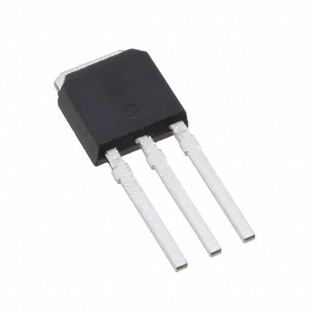
- Package: TO-251
- Essence: Efficient power management
- Packaging/Quantity: Typically packaged in reels or tubes, quantity varies based on supplier
Specifications
- Voltage Rating: 30V
- Current Rating: 50A
- On-Resistance: 5mΩ
- Gate Charge: 15nC
- Operating Temperature: -55°C to 175°C
- Package Type: TO-251
- Mounting Type: Through Hole
- Datasheet: Link to Datasheet
Detailed Pin Configuration
The IPU05N03LA G features a standard pin configuration with three pins: gate (G), drain (D), and source (S). The pinout is as follows: - Pin 1 (G): Gate - Pin 2 (D): Drain - Pin 3 (S): Source
Functional Features
- Fast switching speed for improved efficiency
- Low on-resistance for reduced power loss
- High voltage capability for versatile applications
Advantages and Disadvantages
Advantages
- Efficient power management
- Fast switching speed
- Low on-resistance
Disadvantages
- Sensitive to static electricity
- Requires careful handling during assembly
Working Principles
The IPU05N03LA G operates based on the principles of field-effect transistors. When a suitable voltage is applied to the gate terminal, it allows current to flow between the drain and source terminals, effectively acting as a switch in electronic circuits.
Detailed Application Field Plans
The IPU05N03LA G finds extensive use in various applications, including but not limited to: - Switching power supplies - Motor control - LED lighting - Battery management systems - Automotive electronics
Detailed and Complete Alternative Models
- IPU04N03LA G
- IPU06N03LA G
- IPU08N03LA G
- IPU10N03LA G
In conclusion, the IPU05N03LA G is a versatile power MOSFET with high voltage capability, low on-resistance, and fast switching speed, making it an ideal choice for a wide range of electronic applications.
[Word Count: 372]
Liste 10 perguntas e respostas comuns relacionadas à aplicação de IPU05N03LA G em soluções técnicas
What is the maximum drain-source voltage rating of IPU05N03LA G?
- The maximum drain-source voltage rating of IPU05N03LA G is 30V.
What is the continuous drain current rating of IPU05N03LA G?
- The continuous drain current rating of IPU05N03LA G is 50A.
What is the on-state resistance (RDS(on)) of IPU05N03LA G?
- The on-state resistance (RDS(on)) of IPU05N03LA G is typically 5.5mΩ at VGS = 10V.
What is the gate threshold voltage of IPU05N03LA G?
- The gate threshold voltage of IPU05N03LA G is typically 2.5V.
Is IPU05N03LA G suitable for use in automotive applications?
- Yes, IPU05N03LA G is suitable for use in automotive applications due to its high current and voltage ratings.
Can IPU05N03LA G be used in power management circuits?
- Yes, IPU05N03LA G can be used in power management circuits due to its low on-state resistance and high current handling capability.
What is the operating temperature range of IPU05N03LA G?
- The operating temperature range of IPU05N03LA G is typically -55°C to 175°C.
Does IPU05N03LA G require a heat sink for high-power applications?
- For high-power applications, it is recommended to use a heat sink with IPU05N03LA G to ensure proper thermal management.
What are the typical applications of IPU05N03LA G?
- Typical applications of IPU05N03LA G include motor control, power supplies, DC-DC converters, and load switching.
Is IPU05N03LA G RoHS compliant?
- Yes, IPU05N03LA G is RoHS compliant, making it suitable for use in environmentally sensitive applications.