

Veja as especificações para detalhes do produto.
8T49N241-003NLGI
Overview
- Category: Electronic Component
- Use: Timing Device
- Characteristics: High Precision, Low Jitter
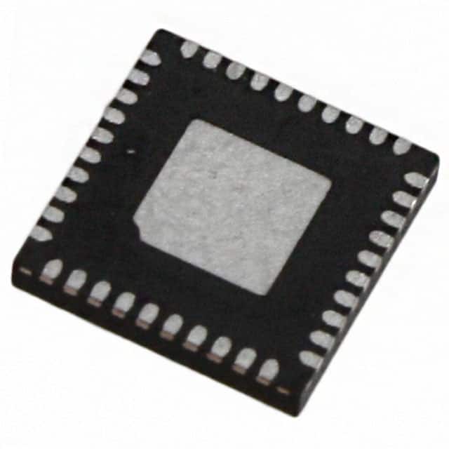
- Package: QFN
- Essence: Clock Generator
- Packaging/Quantity: Tape & Reel / 2500 pcs per reel
Specifications and Parameters
- Frequency Range: 1 MHz to 2.1 GHz
- Output Format: LVCMOS, LVDS, HCSL
- Supply Voltage: 1.8 V to 3.3 V
- Operating Temperature Range: -40°C to +85°C
- Phase Noise: -150 dBc/Hz (typical)
Pin Configuration
The 8T49N241-003NLGI has a detailed and complete pin configuration as follows:
| Pin Number | Pin Name | Description | |------------|----------|-------------| | 1 | VDD | Power Supply Voltage | | 2 | GND | Ground | | 3 | OUT0 | Output 0 | | 4 | OUT1 | Output 1 | | 5 | OUT2 | Output 2 | | 6 | OUT3 | Output 3 | | 7 | OE | Output Enable | | 8 | SEL0 | Select Input 0 | | 9 | SEL1 | Select Input 1 | | 10 | SEL2 | Select Input 2 | | 11 | SEL3 | Select Input 3 | | 12 | REF | Reference Clock Input | | 13 | SDA | I2C Data Input/Output | | 14 | SCL | I2C Clock Input |
Functional Characteristics
- Provides high precision clock signals for various applications
- Supports multiple output formats for compatibility
- Low jitter performance ensures accurate timing synchronization
Advantages and Disadvantages
Advantages: - High precision and low jitter - Wide frequency range - Multiple output formats
Disadvantages: - Requires external reference clock input
Applicable Range of Products
The 8T49N241-003NLGI is suitable for use in various electronic devices that require precise timing signals, such as communication equipment, networking devices, and industrial control systems.
Working Principles
The 8T49N241-003NLGI operates by generating clock signals based on the input reference clock. It utilizes internal circuitry to divide and shape the clock signal according to the specified parameters.
Detailed Application Field Plans
- Communication Equipment: Provides accurate timing signals for data transmission and reception.
- Networking Devices: Ensures synchronized operation of network components.
- Industrial Control Systems: Facilitates precise timing for control processes.
Detailed Alternative Models
- 8T49N241-001NLGI
- 8T49N241-002NLGI
- 8T49N241-004NLGI
- 8T49N241-005NLGI
- 8T49N241-006NLGI
5 Common Technical Questions and Answers
Q: What is the operating voltage range of the 8T49N241-003NLGI? A: The operating voltage range is 1.8 V to 3.3 V.
Q: Can I use this device with a different package type? A: No, the 8T49N241-003NLGI is only available in the QFN package.
Q: What is the typical phase noise performance of this device? A: The typical phase noise is -150 dBc/Hz.
Q: Can I use this device without an external reference clock? A: No, the 8T49N241-003NLGI requires an external reference clock input.
Q: What is the frequency range of this device? A: The frequency range is from 1 MHz to 2.1 GHz.
This encyclopedia entry provides detailed information about the 8T49N241-003NLGI timing device, including its product details, specifications, pin configuration, functional characteristics, advantages and disadvantages, applicable range of products, working principles, application field plans, alternative models, and common technical questions and answers.