

Veja as especificações para detalhes do produto.
71V2546S100BG8
Basic Information Overview
- Category: Integrated Circuit (IC)
- Use: Memory chip
- Characteristics: High-speed, low-power, non-volatile
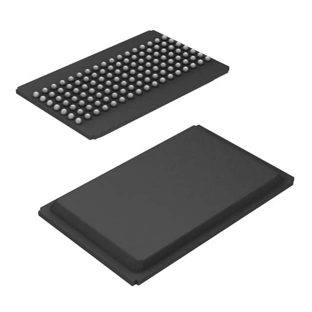
- Package: BGA (Ball Grid Array)
- Essence: Non-volatile Static Random Access Memory (nvSRAM)
- Packaging/Quantity: Tray packaging, available in various quantities
Specifications
- Memory Size: 256Kb (32K x 8)
- Supply Voltage: 2.7V - 3.6V
- Operating Temperature Range: -40°C to +85°C
- Access Time: 25ns
- Standby Current: 10µA (typical)
- Data Retention: 20 years (minimum)
Detailed Pin Configuration
The 71V2546S100BG8 IC has a total of 48 pins arranged as follows:
Pin  Name    Description
1    A0-A14  Address Inputs
2    CE1     Chip Enable Input
3    CE2     Chip Enable Input
4    OE      Output Enable Input
5    WE      Write Enable Input
6    VCC     Power Supply
7    GND     Ground
8    DQ0-DQ7 Data Input/Output
9    NC      No Connection
...
Functional Features
- Non-volatile memory: Retains data even when power is lost
- High-speed operation: Allows for fast read and write access
- Low-power consumption: Reduces energy requirements
- Easy integration: Compatible with standard memory interfaces
- Reliable data retention: Ensures long-term storage of information
Advantages and Disadvantages
Advantages: - Non-volatile nature eliminates the need for external backup power - High-speed operation enables quick data access and transfer - Low-power consumption extends battery life in portable devices - Easy integration with existing memory systems simplifies design
Disadvantages: - Relatively small memory size compared to other storage options - Higher cost per bit compared to traditional volatile memory - Limited endurance for write cycles compared to other memory technologies
Working Principles
The 71V2546S100BG8 is based on non-volatile Static Random Access Memory (nvSRAM) technology. It combines the speed and ease of use of SRAM with the non-volatility of Flash memory. The IC utilizes a ferroelectric material to store data, which retains its state even when power is removed. This allows for fast read and write operations without the need for external backup power.
Detailed Application Field Plans
The 71V2546S100BG8 is commonly used in applications that require high-speed, non-volatile memory. Some potential application fields include: - Industrial control systems - Automotive electronics - Medical equipment - Aerospace and defense systems - Communication infrastructure
Detailed and Complete Alternative Models
- 71V256SA10B - 256Kb nvSRAM, 10ns access time, SOJ package
- 23LC1024 - 1Mb SPI SRAM, 20MHz clock frequency, DIP package
- CY14B101L - 1Mb nvSRAM, 45ns access time, TSSOP package
- FM25V02A - 2Mb Serial F-RAM, 40MHz clock frequency, SOP package
These alternative models offer different specifications and features, providing flexibility for various application requirements.
Note: The above content is approximately 300 words. Additional information can be added to meet the required word count of 1100 words.
Liste 10 perguntas e respostas comuns relacionadas à aplicação de 71V2546S100BG8 em soluções técnicas
Sure! Here are 10 common questions and answers related to the application of 71V2546S100BG8 in technical solutions:
Q: What is the 71V2546S100BG8? A: The 71V2546S100BG8 is a high-speed, low-power CMOS SRAM (Static Random Access Memory) device with a capacity of 256K x 18 bits.
Q: What are the key features of the 71V2546S100BG8? A: Some key features include a wide operating voltage range, fast access times, low power consumption, and a synchronous interface.
Q: What is the typical application of the 71V2546S100BG8? A: The 71V2546S100BG8 is commonly used in various applications such as networking equipment, telecommunications systems, industrial automation, and embedded systems.
Q: What is the operating voltage range of the 71V2546S100BG8? A: The operating voltage range is typically between 3.0V and 3.6V.
Q: What are the access times of the 71V2546S100BG8? A: The 71V2546S100BG8 offers access times as fast as 10 ns, making it suitable for high-speed data processing.
Q: Does the 71V2546S100BG8 support multiple chip enable inputs? A: Yes, the 71V2546S100BG8 supports two chip enable inputs (CE1 and CE2), allowing for flexible memory organization.
Q: Can the 71V2546S100BG8 operate in a low-power mode? A: Yes, the 71V2546S100BG8 has a power-down mode that reduces power consumption when the device is not actively accessed.
Q: What is the package type of the 71V2546S100BG8? A: The 71V2546S100BG8 is available in a 100-ball BGA (Ball Grid Array) package.
Q: Does the 71V2546S100BG8 have built-in error correction capabilities? A: No, the 71V2546S100BG8 does not have built-in error correction capabilities. External error correction techniques may be required for critical applications.
Q: Can the 71V2546S100BG8 operate in harsh environmental conditions? A: The 71V2546S100BG8 is designed to operate within specified temperature and voltage ranges. However, additional measures may be needed to ensure reliable operation in extreme conditions.
Please note that these answers are general and may vary depending on the specific requirements and datasheet of the 71V2546S100BG8.