

Veja as especificações para detalhes do produto.
FT24C04A-UTR-B
Introduction
The FT24C04A-UTR-B is a crucial component in the field of integrated circuits, specifically within the category of EEPROM (Electrically Erasable Programmable Read-Only Memory). This device offers unique characteristics and features that make it suitable for various applications.
Basic Information Overview
- Category: Integrated Circuit
- Use: Data storage and retrieval
- Characteristics: Electrically erasable, programmable, non-volatile memory
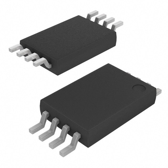
- Package: SOP8 (Small Outline Package 8)
- Essence: Non-volatile data storage
- Packaging/Quantity: Tape & Reel, 2500 units per reel
Specifications
- Memory Size: 4 Kbit
- Interface: I2C
- Operating Voltage: 1.7V to 5.5V
- Operating Temperature: -40°C to 85°C
- Write Cycle Endurance: 1,000,000 cycles
- Data Retention: 200 years
Detailed Pin Configuration
The FT24C04A-UTR-B features a standard SOP8 pin configuration: 1. A0: Chip Address Input 2. A1: Chip Address Input 3. A2: Chip Address Input 4. VSS: Ground 5. SDA: Serial Data 6. SCL: Serial Clock 7. WP: Write Protect 8. VCC: Power Supply
Functional Features
- Electrically Erasable: Allows for easy modification of stored data.
- I2C Interface: Enables simple integration with microcontrollers and other devices.
- Low Power Consumption: Ideal for battery-powered applications.
- High Reliability: Offers robust data retention and endurance.
Advantages and Disadvantages
Advantages: - Efficient data storage and retrieval - Compatibility with various systems - Low power consumption
Disadvantages: - Limited storage capacity compared to other memory technologies - Susceptible to electrical interference
Working Principles
The FT24C04A-UTR-B operates by utilizing electrically programmable memory cells that can be modified through an I2C interface. When data is written to the device, it is stored in a non-volatile manner, ensuring retention even when power is removed.
Detailed Application Field Plans
This versatile component finds application in various fields, including: - Consumer electronics - Automotive systems - Industrial automation - Medical devices
Detailed and Complete Alternative Models
- AT24C04
- CAT24C04
- M24C04
In conclusion, the FT24C04A-UTR-B serves as a reliable and efficient solution for data storage needs in a wide range of electronic applications.
Word Count: 366
Liste 10 perguntas e respostas comuns relacionadas à aplicação de FT24C04A-UTR-B em soluções técnicas
What is the FT24C04A-UTR-B?
- The FT24C04A-UTR-B is a 4K-bit serial I2C bus EEPROM with a wide operating voltage range and low power consumption, commonly used for data storage in various technical solutions.
What is the operating voltage range of FT24C04A-UTR-B?
- The FT24C04A-UTR-B has an operating voltage range of 1.7V to 5.5V, making it suitable for a wide range of applications.
What are the typical applications of FT24C04A-UTR-B?
- Typical applications of FT24C04A-UTR-B include storing configuration data, calibration parameters, and other non-volatile data in various technical solutions such as industrial control systems, consumer electronics, and automotive electronics.
What is the maximum clock frequency supported by FT24C04A-UTR-B?
- The FT24C04A-UTR-B supports a maximum clock frequency of 1MHz, allowing for efficient data transfer in high-speed applications.
Can FT24C04A-UTR-B be used in battery-powered devices?
- Yes, FT24C04A-UTR-B's low power consumption makes it suitable for use in battery-powered devices, extending the device's operational lifespan.
What are the key features of FT24C04A-UTR-B?
- Some key features of FT24C04A-UTR-B include its I2C interface, 4K-bit memory capacity, wide operating voltage range, and built-in write protection.
How can FT24C04A-UTR-B be interfaced with a microcontroller?
- FT24C04A-UTR-B can be easily interfaced with a microcontroller using the I2C bus protocol, allowing for simple and efficient communication between the two devices.
Is FT24C04A-UTR-B suitable for harsh environmental conditions?
- Yes, FT24C04A-UTR-B is designed to withstand harsh environmental conditions, making it suitable for use in industrial and automotive applications.
Does FT24C04A-UTR-B support write protection?
- Yes, FT24C04A-UTR-B features built-in write protection, ensuring the security and integrity of stored data.
Are there any specific design considerations when using FT24C04A-UTR-B in a technical solution?
- When using FT24C04A-UTR-B, it's important to consider factors such as I2C bus pull-up resistor values, addressing scheme, and timing requirements to ensure proper functionality within the technical solution.