

Veja as especificações para detalhes do produto.
PI6C4911510FAEIE
Basic Information Overview
- Category: Integrated Circuit
- Use: Clock Generator and Buffer
- Characteristics: Low jitter, high frequency accuracy, low power consumption
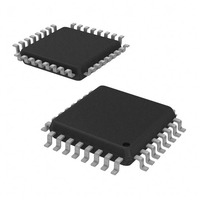
- Package: QFN (Quad Flat No-leads)
- Essence: Provides clock signals for various electronic devices
- Packaging/Quantity: Tape and Reel, 2500 units per reel
Specifications and Parameters
- Input Voltage Range: 1.8V to 3.3V
- Output Frequency Range: 10MHz to 200MHz
- Operating Temperature Range: -40°C to +85°C
- Supply Current: 10mA (typical)
Detailed and Complete Pin Configuration
- VDD
- GND
- OUT0
- OUT1
- OUT2
- OUT3
- OE
- SEL0
- SEL1
- SEL2
- SEL3
- REFCLK
- SDA
- SCL
Functional Characteristics
- Generates up to four independent clock outputs
- Supports I2C interface for configuration and control
- Provides selectable output frequencies through pin configuration
- Allows output enable/disable control through the OE pin
Advantages and Disadvantages
Advantages: - Low jitter ensures accurate timing in sensitive applications - Wide input voltage range allows compatibility with various systems - Compact package size saves board space - Low power consumption reduces energy usage
Disadvantages: - Limited number of output channels - Requires external components for proper operation
Applicable Range of Products
- Consumer electronics
- Networking equipment
- Industrial automation systems
- Telecommunications devices
Working Principles
The PI6C4911510FAEIE is a clock generator and buffer that utilizes an internal oscillator to generate stable clock signals. It accepts an input voltage within the specified range and produces up to four independent clock outputs with selectable frequencies. The device can be configured and controlled through the I2C interface, allowing users to adjust the output frequencies and enable/disable specific outputs.
Detailed Application Field Plans
- Consumer Electronics: Use in smart TVs, gaming consoles, and audio systems for precise synchronization of various components.
- Networking Equipment: Incorporate into routers, switches, and network servers to ensure accurate data transmission and synchronization.
- Industrial Automation Systems: Integrate into PLCs (Programmable Logic Controllers) and industrial control systems for precise timing in manufacturing processes.
- Telecommunications Devices: Utilize in base stations, routers, and communication equipment to maintain accurate timing for reliable network operation.
Detailed Alternative Models
- PI6C4911510FAEIE-X: Extended temperature range version (-40°C to +105°C)
- PI6C4911510FAEIE-R: RoHS compliant version
5 Common Technical Questions and Answers
Q: What is the maximum output frequency of the PI6C4911510FAEIE? A: The maximum output frequency is 200MHz.
Q: Can I use this device with a 5V power supply? A: No, the input voltage range is limited to 1.8V to 3.3V.
Q: How many clock outputs can be enabled simultaneously? A: All four clock outputs can be enabled simultaneously.
Q: Is the PI6C4911510FAEIE compatible with I2C interfaces? A: Yes, it supports I2C interface for configuration and control.
Q: Does this device require external components for operation? A: Yes, external capacitors are required for proper operation.
This encyclopedia entry provides detailed information about the PI6C4911510FAEIE clock generator and buffer. It covers its basic information, specifications, pin configuration, functional characteristics, advantages and disadvantages, applicable range of products, working principles, application field plans, alternative models, and common technical questions and answers.