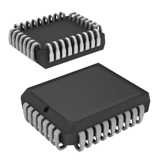
Veja as especificações para detalhes do produto.

CY7C4261-15JXC
Product Overview
Category
CY7C4261-15JXC belongs to the category of high-speed synchronous SRAM (Static Random Access Memory) chips.
Use
This product is primarily used in applications that require fast and reliable data storage and retrieval. It is commonly employed in various electronic devices such as computers, servers, networking equipment, and telecommunications systems.
Characteristics
- High Speed: The CY7C4261-15JXC operates at a clock frequency of 133 MHz, allowing for rapid data access.
- Large Capacity: With a capacity of 4 Megabits (512K x 8), this SRAM chip provides ample storage space for data-intensive applications.
- Low Power Consumption: The device is designed to minimize power consumption, making it suitable for battery-powered devices.
- Asynchronous and Synchronous Operation: The CY7C4261-15JXC supports both asynchronous and synchronous operation modes, providing flexibility in different system configurations.
Package
The CY7C4261-15JXC is available in a compact and industry-standard 32-pin PLCC (Plastic Leaded Chip Carrier) package. This package offers ease of integration into various circuit board designs.
Essence
The essence of the CY7C4261-15JXC lies in its ability to provide high-speed and reliable data storage, enabling efficient processing and execution of tasks in electronic systems.
Packaging/Quantity
This product is typically packaged in reels or tubes, with each containing a specific quantity of CY7C4261-15JXC chips. The exact packaging and quantity may vary depending on the supplier and customer requirements.
Specifications
- Organization: 512K x 8 bits
- Operating Voltage: 3.3V
- Clock Frequency: 133 MHz
- Access Time: 15 ns
- Operating Temperature Range: -40°C to +85°C
- Data Retention Voltage: 2.0V (min)
- Package Type: 32-pin PLCC
Detailed Pin Configuration
The CY7C4261-15JXC features a total of 32 pins, each serving a specific function in the device's operation. The pin configuration is as follows:
```
Pin Name Description
1 Vcc Power Supply 2 A12 Address Input 3 A7 Address Input 4 A6 Address Input 5 A5 Address Input 6 A4 Address Input 7 A3 Address Input 8 A2 Address Input 9 A1 Address Input 10 A0 Address Input 11 DQ0 Data Input/Output 12 DQ1 Data Input/Output 13 DQ2 Data Input/Output 14 DQ3 Data Input/Output 15 DQ4 Data Input/Output 16 DQ5 Data Input/Output 17 DQ6 Data Input/Output 18 DQ7 Data Input/Output 19 GND Ground 20 WE# Write Enable 21 CE# Chip Enable 22 OE# Output Enable 23 UB/LB# Upper Byte/Lower Byte Control 24 A8 Address Input 25 A9 Address Input 26 A11 Address Input 27 A10 Address Input 28 A15 Address Input 29 A14 Address Input 30 A13 Address Input 31 NC No Connection 32 Vcc Power Supply ```
Functional Features
- High-Speed Operation: The CY7C4261-15JXC offers fast access times, allowing for efficient data retrieval and storage.
- Asynchronous and Synchronous Modes: The device supports both asynchronous and synchronous operation, providing compatibility with different system architectures.
- Low Power Consumption: This SRAM chip is designed to minimize power consumption, making it suitable for energy-efficient applications.
- Easy Integration: The industry-standard package and pin configuration facilitate seamless integration into various circuit board designs.
Advantages and Disadvantages
Advantages
- High-speed operation enables rapid data access.
- Large capacity provides ample storage space for data-intensive applications.
- Low power consumption prolongs battery life in portable devices.
- Compatibility with both asynchronous and synchronous modes allows for flexible system configurations.
- Easy integration due to the standard package and pin configuration.
Disadvantages
- Limited availability of alternative models may restrict design options.
- Relatively higher cost compared to other memory technologies.
Working Principles
The CY7C4261-15JXC operates based on the principles of static random access memory. It utilizes flip-flops to store and retrieve data. When a read or write operation is initiated,
Liste 10 perguntas e respostas comuns relacionadas à aplicação de CY7C4261-15JXC em soluções técnicas
Sure! Here are 10 common questions and answers related to the application of CY7C4261-15JXC in technical solutions:
Q1: What is the CY7C4261-15JXC? A1: The CY7C4261-15JXC is a specific model of synchronous SRAM (Static Random Access Memory) chip manufactured by Cypress Semiconductor.
Q2: What is the operating voltage range for CY7C4261-15JXC? A2: The operating voltage range for CY7C4261-15JXC is typically between 3.0V and 3.6V.
Q3: What is the capacity of CY7C4261-15JXC? A3: The CY7C4261-15JXC has a capacity of 256 kilobits (32 kilobytes).
Q4: What is the access time of CY7C4261-15JXC? A4: The access time of CY7C4261-15JXC is 15 nanoseconds (ns).
Q5: Can CY7C4261-15JXC be used in battery-powered devices? A5: Yes, CY7C4261-15JXC can be used in battery-powered devices as it operates within a low voltage range.
Q6: Is CY7C4261-15JXC compatible with different microcontrollers? A6: Yes, CY7C4261-15JXC is compatible with various microcontrollers that support synchronous SRAM interfaces.
Q7: Can CY7C4261-15JXC be used in industrial applications? A7: Yes, CY7C4261-15JXC is suitable for industrial applications due to its robust design and wide operating temperature range.
Q8: Does CY7C4261-15JXC support burst mode operation? A8: Yes, CY7C4261-15JXC supports burst mode operation, allowing for faster data transfer rates.
Q9: Can multiple CY7C4261-15JXC chips be cascaded together? A9: Yes, multiple CY7C4261-15JXC chips can be cascaded together to increase the overall memory capacity.
Q10: Are there any specific design considerations when using CY7C4261-15JXC? A10: Yes, it is important to ensure proper decoupling and signal integrity measures while designing the PCB layout for CY7C4261-15JXC-based solutions.
Please note that these answers are general and may vary depending on the specific requirements and application of CY7C4261-15JXC in a technical solution.

