

Veja as especificações para detalhes do produto.
CY7C4225V-15ASXCT
Product Overview
Category
The CY7C4225V-15ASXCT belongs to the category of integrated circuits (ICs), specifically a synchronous dual-port static random access memory (SDP SRAM) chip.
Use
This IC is primarily used in applications that require high-speed and reliable data storage and retrieval. It provides simultaneous access to two independent ports, making it suitable for multi-processor systems, networking equipment, and other high-performance computing devices.
Characteristics
- Synchronous operation: The CY7C4225V-15ASXCT operates synchronously with an external clock signal, ensuring precise timing and efficient data transfer.
- Dual-port architecture: It features two separate ports, allowing simultaneous read and write operations from different sources.
- High-speed performance: With a maximum operating frequency of 150 MHz, this IC offers fast data access and transfer rates.
- Low power consumption: The CY7C4225V-15ASXCT is designed to minimize power consumption, making it suitable for battery-powered devices.
- Wide voltage range: It supports a wide supply voltage range of 3.0V to 3.6V, providing flexibility in various system configurations.
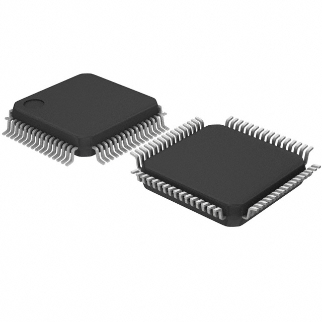
Package and Quantity
The CY7C4225V-15ASXCT is available in a small-outline integrated circuit (SOIC) package. Each package contains one IC.
Specifications
- Organization: 256K x 18 bits
- Access time: 15 ns
- Operating voltage: 3.0V - 3.6V
- Operating temperature range: -40°C to +85°C
- Package type: SOIC
- Pin count: 48
Detailed Pin Configuration
The CY7C4225V-15ASXCT has a total of 48 pins. Here is a detailed pin configuration:
- VDDQ
- DQ0
- DQ1
- DQ2
- DQ3
- DQ4
- DQ5
- DQ6
- DQ7
- DQ8
- DQ9
- DQ10
- DQ11
- DQ12
- DQ13
- DQ14
- DQ15
- DQ16
- DQ17
- DQ18
- DQ19
- DQ20
- DQ21
- DQ22
- DQ23
- GND
- A0
- A1
- A2
- A3
- A4
- A5
- A6
- A7
- A8
- A9
- A10
- A11
- A12
- A13
- A14
- A15
- A16
- A17
- A18
- A19
- WE
- OE
Functional Features
- Simultaneous read and write: The dual-port architecture allows independent read and write operations to occur simultaneously, enhancing system performance.
- Asynchronous and synchronous operation: The CY7C4225V-15ASXCT supports both asynchronous and synchronous modes of operation, providing flexibility in different system configurations.
- Byte-write capability: It allows individual bytes within a word to be written independently, enabling efficient memory utilization.
- Automatic power-down: This IC features an automatic power-down mode to conserve energy when not in use.
Advantages
- High-speed operation: The CY7C4225V-15ASXCT offers fast access times and data transfer rates, improving overall system performance.
- Dual-port architecture: Simultaneous access to two independent ports enables efficient data exchange between different components of a system.
- Low power consumption: With its low power design, this IC is suitable for battery-powered devices and energy-efficient applications.
- Wide voltage range: The ability to operate within a wide voltage range provides compatibility with various system configurations.
Disadvantages
- Limited storage capacity: The CY7C4225V-15ASXCT has a specific memory size (256K x 18 bits), which may not be sufficient for certain high-capacity storage requirements.
- Cost: As an integrated circuit with advanced features, the CY7C4225V-15ASXCT may have a higher cost compared to simpler memory chips.
Working Principles
The CY7C4225V-15ASXCT operates by storing data in its static random access memory cells. It utilizes synchronous operation, where data transfers occur in synchronization with an external clock signal. The dual-port architecture allows simultaneous read and
Liste 10 perguntas e respostas comuns relacionadas à aplicação de CY7C4225V-15ASXCT em soluções técnicas
Sure! Here are 10 common questions and answers related to the application of CY7C4225V-15ASXCT in technical solutions:
Question: What is the maximum operating frequency of CY7C4225V-15ASXCT?
Answer: The maximum operating frequency of CY7C4225V-15ASXCT is 133 MHz.Question: What is the voltage supply range for CY7C4225V-15ASXCT?
Answer: CY7C4225V-15ASXCT operates with a voltage supply range of 3.0V to 3.6V.Question: Can CY7C4225V-15ASXCT be used in industrial applications?
Answer: Yes, CY7C4225V-15ASXCT is suitable for industrial applications due to its wide temperature range and robust design.Question: Does CY7C4225V-15ASXCT support multiple memory banks?
Answer: No, CY7C4225V-15ASXCT is a single memory bank device.Question: What is the capacity of CY7C4225V-15ASXCT?
Answer: CY7C4225V-15ASXCT has a capacity of 256K x 18 bits.Question: Can CY7C4225V-15ASXCT operate at different speeds?
Answer: Yes, CY7C4225V-15ASXCT supports various speed grades, including 10 ns, 12 ns, and 15 ns.Question: Is CY7C4225V-15ASXCT compatible with other memory devices?
Answer: Yes, CY7C4225V-15ASXCT is compatible with other SRAM devices and can be used in conjunction with them.Question: Does CY7C4225V-15ASXCT have any power-saving features?
Answer: Yes, CY7C4225V-15ASXCT supports various power-saving modes to reduce power consumption when not in use.Question: Can CY7C4225V-15ASXCT be used in battery-powered applications?
Answer: Yes, CY7C4225V-15ASXCT's low power consumption makes it suitable for battery-powered applications.Question: What is the package type of CY7C4225V-15ASXCT?
Answer: CY7C4225V-15ASXCT is available in a 100-pin TQFP (Thin Quad Flat Package) package.
Please note that these answers are based on general information about CY7C4225V-15ASXCT and may vary depending on specific application requirements.