

Veja as especificações para detalhes do produto.
ADCMP572BCPZ-R2
Product Overview
Category: Analog-to-Digital Converter (ADC)
Use: The ADCMP572BCPZ-R2 is a high-speed, low-power, 12-bit analog-to-digital converter designed for various applications in the field of signal processing and data acquisition. It provides accurate conversion of analog signals into digital format.
Characteristics: - High-speed conversion with a sampling rate of up to 100 MSPS (Mega Samples Per Second) - Low power consumption, making it suitable for portable and battery-powered devices - 12-bit resolution for precise and detailed digital representation of analog signals - Wide input voltage range, allowing compatibility with different signal sources - Integrated features for enhanced performance, such as programmable gain amplifier and reference voltage generator
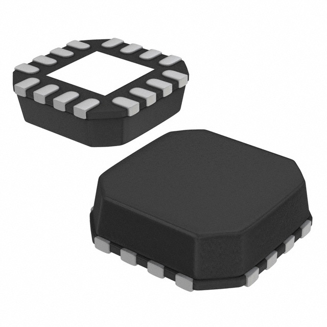
Package: The ADCMP572BCPZ-R2 is available in a compact and industry-standard LFCSP (Lead Frame Chip Scale Package) package. This package ensures easy integration into various circuit designs and provides reliable electrical connections.
Essence: The essence of the ADCMP572BCPZ-R2 lies in its ability to accurately convert analog signals into digital format, enabling further processing and analysis of the acquired data.
Packaging/Quantity: The ADCMP572BCPZ-R2 is typically sold in reels or trays, containing a specific quantity of units per package. The exact packaging and quantity may vary depending on the supplier.
Specifications
- Resolution: 12 bits
- Sampling Rate: Up to 100 MSPS
- Input Voltage Range: ±1 V
- Power Supply: 3.3 V
- Power Consumption: 150 mW (typical)
- Operating Temperature Range: -40°C to +85°C
- Package Type: LFCSP
Detailed Pin Configuration
The ADCMP572BCPZ-R2 has a total of 32 pins, each serving a specific function. The pin configuration is as follows:
- VREFP: Positive reference voltage input
- VREFN: Negative reference voltage input
- AGND: Analog ground
- VIN: Analog input voltage
- VCM: Common-mode voltage input
- CLK: Clock input
- CS: Chip select input
- SDO: Serial data output
- SDI: Serial data input
- DGND: Digital ground
- DVDD: Digital power supply 12-19. D[11:4]: Data output bits
- D[3]: Data output bit
- D[2]: Data output bit
- D[1]: Data output bit
- D[0]: Data output bit
- PDWN: Power-down control input
- RESET: Reset control input
- REFOUT: Reference voltage output
- AVDD: Analog power supply
- VBIAS: Bias voltage input
- VCMO: Common-mode voltage output
- VREFM: Mid-scale reference voltage output
- VREFB: Buffer reference voltage output
- VREFG: Gain reference voltage output
Functional Features
The ADCMP572BCPZ-R2 offers several functional features that enhance its performance and usability:
- Programmable Gain Amplifier (PGA): The integrated PGA allows users to adjust the gain of the input signal, enabling amplification or attenuation as required.
- Reference Voltage Generator: The built-in reference voltage generator provides stable and accurate reference voltages for the ADC, ensuring precise conversion.
- Serial Data Interface: The ADCMP572BCPZ-R2 utilizes a serial data interface (SDI and SDO pins) for easy integration with microcontrollers or other digital devices.
- Power-Down Mode: The power-down control input (PDWN) allows the ADC to enter a low-power state when not in use, conserving energy and extending battery life.
Advantages and Disadvantages
Advantages: - High-speed conversion enables real-time signal processing - Low power consumption makes it suitable for portable devices - Wide input voltage range provides flexibility in signal source selection - Integrated features enhance performance and simplify circuit design
Disadvantages: - Limited resolution compared to higher-end ADCs - May require additional external components for specific applications - Higher cost compared to lower-performance ADCs
Working Principles
The ADCMP572BCPZ-R2 operates on the principle of successive approximation. It samples the analog input voltage at a high rate and compares it to a reference voltage. By iteratively adjusting the digital representation of the input voltage, it converges to a digital value that accurately represents the analog signal.
Detailed Application Field Plans
The ADCMP572BCPZ-R2 finds applications in various fields where accurate analog-to-digital conversion is required.
Liste 10 perguntas e respostas comuns relacionadas à aplicação de ADCMP572BCPZ-R2 em soluções técnicas
Sure! Here are 10 common questions and answers related to the application of ADCMP572BCPZ-R2 in technical solutions:
Q: What is the ADCMP572BCPZ-R2? A: The ADCMP572BCPZ-R2 is a high-speed comparator IC (integrated circuit) used for precision signal detection and measurement.
Q: What is the operating voltage range of ADCMP572BCPZ-R2? A: The ADCMP572BCPZ-R2 operates within a voltage range of 2.7V to 5.5V.
Q: What is the maximum input voltage that ADCMP572BCPZ-R2 can handle? A: The ADCMP572BCPZ-R2 can handle input voltages up to 5.5V.
Q: What is the typical response time of ADCMP572BCPZ-R2? A: The typical response time of ADCMP572BCPZ-R2 is around 3 ns.
Q: Can ADCMP572BCPZ-R2 be used in high-frequency applications? A: Yes, ADCMP572BCPZ-R2 is suitable for high-frequency applications as it has a wide bandwidth of 1 GHz.
Q: Does ADCMP572BCPZ-R2 have built-in hysteresis? A: Yes, ADCMP572BCPZ-R2 features built-in hysteresis to provide noise immunity and prevent false triggering.
Q: What is the power supply current consumption of ADCMP572BCPZ-R2? A: The power supply current consumption of ADCMP572BCPZ-R2 is typically 3.5 mA.
Q: Can ADCMP572BCPZ-R2 operate in harsh environments? A: Yes, ADCMP572BCPZ-R2 is designed to operate in a wide temperature range (-40°C to +125°C) and is suitable for harsh environments.
Q: What are the available package options for ADCMP572BCPZ-R2? A: ADCMP572BCPZ-R2 is available in a small footprint 8-lead LFCSP (lead-frame chip-scale package).
Q: What are some typical applications of ADCMP572BCPZ-R2? A: ADCMP572BCPZ-R2 is commonly used in applications such as high-speed data acquisition, communications systems, test and measurement equipment, and industrial automation.
Please note that these answers are general and may vary depending on specific datasheet specifications and application requirements.