

Veja as especificações para detalhes do produto.
AS6C1016-55BIN
Product Overview
Category
AS6C1016-55BIN belongs to the category of semiconductor memory devices.
Use
It is primarily used for data storage and retrieval in electronic devices such as computers, smartphones, and embedded systems.
Characteristics
- High-speed operation
- Low power consumption
- Non-volatile storage
- Compact size
Package
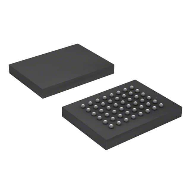
AS6C1016-55BIN is available in a small outline integrated circuit (SOIC) package.
Essence
The essence of AS6C1016-55BIN lies in its ability to store and retrieve digital information reliably and efficiently.
Packaging/Quantity
AS6C1016-55BIN is typically packaged in reels or trays, with each reel containing a specific quantity of chips. The exact packaging and quantity may vary depending on the manufacturer.
Specifications
- Memory Capacity: 1 Megabit (128K x 8 bits)
- Operating Voltage: 2.7V - 5.5V
- Access Time: 55 nanoseconds
- Data Retention: Up to 10 years
- Operating Temperature Range: -40°C to +85°C
Detailed Pin Configuration
AS6C1016-55BIN has a total of 28 pins, which are assigned specific functions. The pin configuration is as follows:
- A0-A16: Address Inputs
- DQ0-DQ7: Data Inputs/Outputs
- WE: Write Enable
- OE: Output Enable
- CE: Chip Enable
- VCC: Power Supply
- GND: Ground
Functional Features
- Random access memory (RAM) functionality
- Byte-wide data organization
- Easy interfacing with microcontrollers and other digital devices
- Low standby current consumption
- Automatic power-down mode for further power savings
Advantages and Disadvantages
Advantages
- High-speed operation enables quick data access
- Low power consumption prolongs battery life in portable devices
- Non-volatile storage ensures data retention even during power loss
- Compact size allows for integration into space-constrained designs
Disadvantages
- Limited storage capacity compared to other memory technologies
- Relatively higher cost per unit compared to alternative memory options
Working Principles
AS6C1016-55BIN operates based on the principles of semiconductor memory technology. It utilizes a combination of transistors and capacitors to store and retrieve digital information. The memory cells within the chip are organized in a grid-like structure, with each cell representing a single bit of data.
Detailed Application Field Plans
AS6C1016-55BIN finds applications in various electronic devices and systems, including but not limited to: - Personal computers - Laptops and notebooks - Mobile phones and smartphones - Tablets and handheld devices - Automotive electronics - Industrial control systems - Medical equipment - Consumer electronics
Detailed and Complete Alternative Models
Some alternative models that offer similar functionality to AS6C1016-55BIN include: - AS6C1008-55BIN - AS6C2008-55BIN - AS6C4008-55BIN - AS6C8008-55BIN
These alternative models differ in terms of memory capacity, but share similar specifications and features.
In conclusion, AS6C1016-55BIN is a high-speed, low-power semiconductor memory device primarily used for data storage and retrieval in various electronic devices. Its compact size, non-volatile storage, and easy interfacing make it suitable for a wide range of applications. While it has certain limitations in terms of storage capacity and cost, it offers advantages such as fast operation and low power consumption.
Liste 10 perguntas e respostas comuns relacionadas à aplicação de AS6C1016-55BIN em soluções técnicas
Sure! Here are 10 common questions and answers related to the application of AS6C1016-55BIN in technical solutions:
Question: What is AS6C1016-55BIN?
- Answer: AS6C1016-55BIN is a specific model of SRAM (Static Random Access Memory) chip.Question: What is the capacity of AS6C1016-55BIN?
- Answer: AS6C1016-55BIN has a capacity of 1 megabit, which is equivalent to 128 kilobytes.Question: What is the operating voltage range for AS6C1016-55BIN?
- Answer: The operating voltage range for AS6C1016-55BIN is typically between 4.5V and 5.5V.Question: What is the access time of AS6C1016-55BIN?
- Answer: AS6C1016-55BIN has an access time of 55 nanoseconds, hence the "55" in its part number.Question: Can AS6C1016-55BIN be used in battery-powered devices?
- Answer: Yes, AS6C1016-55BIN can be used in battery-powered devices as long as the operating voltage range is within the device's power supply capabilities.Question: What is the package type of AS6C1016-55BIN?
- Answer: AS6C1016-55BIN comes in a 44-pin TSOP (Thin Small Outline Package).Question: Is AS6C1016-55BIN compatible with other memory chips?
- Answer: AS6C1016-55BIN is compatible with other SRAM chips that have similar specifications and pinouts.Question: Can AS6C1016-55BIN be used in industrial applications?
- Answer: Yes, AS6C1016-55BIN is suitable for use in industrial applications due to its wide operating temperature range and reliability.Question: What are some typical applications of AS6C1016-55BIN?
- Answer: AS6C1016-55BIN can be used in various applications such as embedded systems, telecommunications equipment, networking devices, and automotive electronics.Question: Where can I find more information about AS6C1016-55BIN?
- Answer: You can refer to the datasheet or contact the manufacturer for more detailed information about AS6C1016-55BIN, including electrical characteristics, timing diagrams, and recommended usage guidelines.