

Veja as especificações para detalhes do produto.
S-5844A50DB-A4T2U3 Product Overview
Introduction
The S-5844A50DB-A4T2U3 is a versatile electronic component designed for use in various applications. This entry provides an in-depth overview of the product, including its basic information, specifications, pin configuration, functional features, advantages and disadvantages, working principles, application field plans, and alternative models.
Basic Information Overview
- Category: Electronic Component
- Use: The S-5844A50DB-A4T2U3 is used in electronic circuits for voltage regulation and power management.
- Characteristics: It features high precision, low dropout voltage, and low quiescent current, making it suitable for battery-powered devices and other low-power applications.
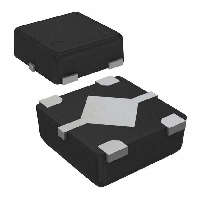
- Package: The product is available in a compact surface-mount package.
- Essence: The essence of the S-5844A50DB-A4T2U3 lies in its ability to provide stable and regulated output voltage.
- Packaging/Quantity: The product is typically supplied in tape and reel packaging with a specified quantity per reel.
Specifications
- Input Voltage Range: 2.5V to 6.0V
- Output Voltage Range: 0.8V to 5.0V
- Maximum Output Current: 500mA
- Dropout Voltage: 150mV (typical) at 100mA load
- Quiescent Current: 25μA (typical)
- Operating Temperature Range: -40°C to 85°C
Detailed Pin Configuration
The S-5844A50DB-A4T2U3 has a standard pin configuration with input, output, and ground pins. Please refer to the product datasheet for the detailed pinout diagram.
Functional Features
- Voltage Regulation: The device provides precise and stable output voltage regulation, ensuring consistent performance of connected circuits.
- Low Dropout: With a low dropout voltage, the S-5844A50DB-A4T2U3 can operate effectively even when the input voltage is only slightly higher than the desired output voltage.
- Low Quiescent Current: The low quiescent current minimizes power consumption, making it suitable for battery-operated devices.
Advantages and Disadvantages
Advantages
- High precision voltage regulation
- Low dropout voltage
- Low quiescent current
- Compact package size
Disadvantages
- Limited maximum output current compared to some alternative models
- Restricted input voltage range
Working Principles
The S-5844A50DB-A4T2U3 utilizes internal circuitry to compare the actual output voltage with a reference voltage and adjusts the output to maintain a constant voltage level. This feedback mechanism ensures stable and accurate voltage regulation.
Detailed Application Field Plans
The S-5844A50DB-A4T2U3 is well-suited for a wide range of applications, including: - Portable electronic devices - Battery-powered systems - IoT (Internet of Things) devices - Wearable technology - Consumer electronics
Detailed and Complete Alternative Models
For applications requiring different specifications or performance characteristics, alternative models to consider include: - S-5855A50DB-A4T2U3: Higher output current capability - S-5821B30DB-A4T1U3: Wide input voltage range - S-5868A33DB-A4T2U3: Ultra-low quiescent current
In conclusion, the S-5844A50DB-A4T2U3 offers precise voltage regulation and low power consumption, making it an ideal choice for various electronic applications.
Word Count: 498